Single crystalline substrates are typically differentiated by the process by which they are made. Czochralski (Cz)[1] wafers are the most commonly used type of silicon wafer, and are used by both the solar and integrated circuit industry. The process of making a large single crystalline silicon ingot by the Czochralski process is shown below. The use of quartz crucibles in the manufacture of Cz substrates causes the incorporation of ppm (1018 cm-3) oxygen into the silicon ingot. The oxygen itself is relatively benign but creates complexes with boron doping that degrades the carrier lifetime.[2][3][4] N-type ingots fabricated with phosphorous dopants have similar oxygen concentrations but do not show the degradation effect nor do wafers with lower resistivity or gallium dopants. [5]
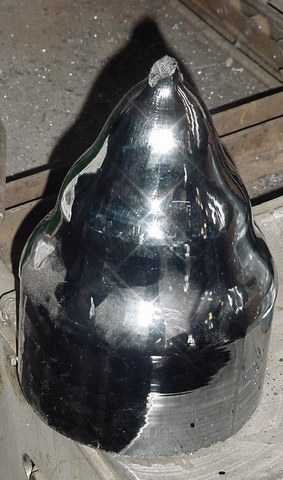
Top of Czochralski ingot. The bottom cylindrical section has been cut off to make wafers. Such "tops and tails" left over from growing the semiconductor industry are a large source of silicon supply for the photovoltaics industry.
- 1. , “Ein neues Verfahren zur Messung der Kristallisationsgeschwindigheit der Metalle”, Zeitschrift für physikalische Chemie, vol. 92, pp. 219–221, 1918.
- 2. Citekey not found
- 3. , “Degradation of carrier lifetime in Cz silicon solar cells”, Solar Energy Materials and Solar Cells, vol. 65, pp. 219 - 229, 2001.
- 4. , “Fundamental boron-oxygen-related carrier lifetime limit in mono- and multicrystalline silicon”, Progress in Photovoltaics: Research and Applications, vol. 13, pp. 287 - 296, 2005.
- 5. , “24.5% efficiency PERT silicon solar cells on SEH MCZ substrates and cell performance on other SEH CZ and FZ substrates”, Solar Energy Materials and Solar Cells, vol. 66, pp. 27 - 36, 2001.